| Sponsor |

|
TIM1 for EV Battery Thermal Management
AIT's thermal adhesives, grease-gels, & gum-pads offer proven thermal dissipation for a balance of strength, rework ability, & recyclability of EV battery packs.
AI Technology, Inc.
|
|
| Technical Paper |
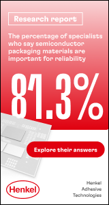
Peer viewpoint: AI data centers are driving a semiconductor revolution
AI adoption is tripling data center demand by 2030. Henkel surveyed 120 semiconductor leaders to uncover how innovation in materials and packaging is powering future-ready, high-performance infrastructure.
Henkel Ltd
Complete this form to download this Technical Paper.
|
|
|
|
More Technical Papers
Full Technical Paper List
|
Free Newsletter Subscription
Semiconductor Packaging News is built for professionals who bear the responsibility of looking ahead, imagining the future, and preparing for it.
Insert Your Email Address
|
| Sponsor |

|
EZ-FLO High Precision Dispense Tips
Each needle is machined from solid stainless steel as opposed to rolled tubing. The resulting smoother internal profile enhances material flow and consistency. Learn more.
DL Technology
|
|
|