Medical Grade, Toughened Epoxy
Master Bond Supreme 121AOMed is a thermally conductive, electrically insulating adhesive that resists repeated autoclaving and is used for bonding, sealing and encapsulation. Master Bond
Technical Paper
Ultrasonic Bonding in semiconductor industry – The fast and clean process
Ultrasonic die bonding revolutionizes semiconductor assembly with rapid processing, strong bonds, and low thermal stress. It excels in bonding dissimilar materials, advancing applications like power devices, RF components, and 3D packaging in modern electronics.
Tresky GmbH
Complete this form to download this Technical Paper.
Free Newsletter Subscription
Semiconductor Packaging News is built for professionals who bear the responsibility of looking ahead, imagining the future, and preparing for it.
Insert Your Email Address
Sponsor
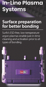
High Capacity & Power Plasma Systems
The BT-1 high capacity plasma systems features 5 shelves & high power plasma up to 5000 watts! Reactive Ion Etching chamber configurations with liquid cooling are also available. Plasma Etch