| Sponsor |

|
Medical Grade, Toughened Epoxy
Master Bond Supreme 121AOMed is a thermally conductive, electrically insulating adhesive that resists repeated autoclaving and is used for bonding, sealing and encapsulation.
Master Bond
|
|
| Viewpoint |
February 17, 2020
VIEWPOINT 2020: John Park, Product Management Group Director, Cadence

|
|
John Park, Product Management Group Director, IC Packaging and Cross-platform Solutions, Cadence
|
As more semiconductor companies look for alternatives to Moore’s Law scaling and begin to fully realize the benefits of modern-day multi-chip(let) packaging (including stacking), expect to see a dramatic reduction in single monolithic SoC design starts. Instead, expect 2020 to launch the age of "More Than Moore", namely multi-chip(let) packaging.
Foundries and OSATs will continue to battle for market share, driving cost (the key metric) lower for state-of-the-art multi-chip(let) packaging. This will greatly accelerate the transition to multi-chip(let) packaging and heterogeneous systems as an alternative to CMOS scaling.
The evolution of Moore's Law is about more than just the limitations of physics. Chasing the latest design node is expensive, hard and requires large design teams. Big chips typically don't yield very well either. Fewer and fewer companies want to take on these challenges when a viable alternative in packaging is so readily available.
John Park, Product Management Group Director, IC Packaging and Cross-platform Solutions
Cadence
http://www.cadence.com
|
Free Newsletter Subscription
Semiconductor Packaging News is built for professionals who bear the responsibility of looking ahead, imagining the future, and preparing for it.
Insert Your Email Address
|
| Sponsor |

|
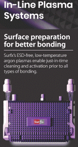
High Capacity & Power Plasma Systems
The BT-1 high capacity plasma systems features 5 shelves & high power plasma up to 5000 watts! Reactive Ion Etching chamber configurations with liquid cooling are also available.
Plasma Etch
|
|
|